Ask our team:
  • Phone: +86 181 0690 9650
  • E-Mail sales1@apterpower.com
  • Lifecycle status

    Active / Available from OEM
    Apter Power accepts quotation requests for DS200TCQAG1A and can provide verified General Electric documentation for its TCQA signal paths.

DS200TCQAG1A

/ 4.9
1001 reviews | Need a Specific Revision?
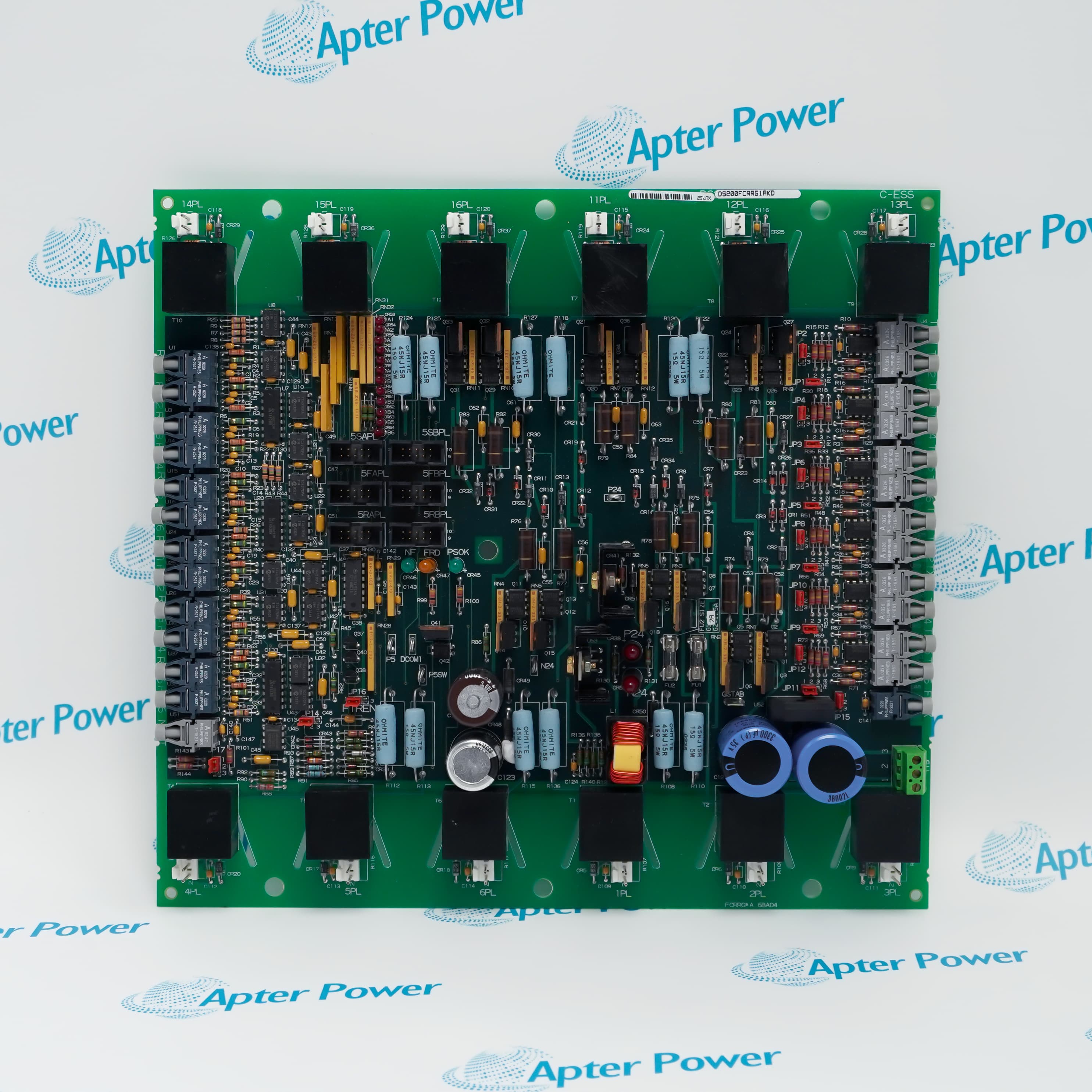
General Electric DS200TCQAG1A is the TCQA analog I/O board that conditions turbine measurements and actuator signals across the Mark V R1, R2, and R3 cores.
In Stock
Ships by Thursday, October 29
Fast Shipping Available
Get a quick price for DS200TCQAG1A
Quantity
*E-mail
Company
*Mobile
*Content
Upload (gif, jpg, jpeg, png, bmp, doc, docx, xls, xlsx, ppt, pdf, csv)

Technical specifications for DS200TCQAG1A

  • Manufacturer:
    General Electric
  • Part Number:
    DS200TCQAG1A
  • Product Family:
    GE Mark V/VI Driver Board
  • Product Type:
    Analog I/O Board
  • Stock:
    1
  • Core Placement:
    R1, R2, and R3 I/O cores
  • Signal Families:
    Thermocouple, LVDT/LVDR, 4–20 mA, vibration, pulse, and voltage
  • Command Outputs:
    Servo-valve, relay-driver, and current-loop paths
  • Core Data Bus:
    3PL to STCA, TCQA, and TCQE
  • Milliamp Circuit Selection:
    J1 and J2 jumpers
  • Output Current Range:
    20 mA or 200 mA via J5 and J6
  • Configuration Tool:
    Mark V I/O Configuration Editor
  • Tariff Code:
    8538900000
  • Country of origin:
    USA
  • Place of shipment:
    Xiamen,Fujian,China
By purchasing this item, you agree to the Terms & Conditions, ApterPower is not an authorized distributor for listed manufacturers or tradenames and therefore the manufacturer's warranty does not apply. All our products come with ApterPower's 1-year warranty.

More Information

Overview Manuals Signal Conditioning Core Connections Diagnostic Context Product Applications

Features:

  • Installed in the R1, R2, and R3 Mark V I/O cores for three-core analog signal conditioning.
  • Separates thermocouple, position, current, vibration, voltage, speed, and actuator circuits through dedicated connectors.
  • Uses board jumpers to assign milliamp output circuits and select the documented 20 mA or 200 mA range.
The DS200TCQAG1A combines acquisition and output functions that would otherwise require several independent interfaces. Its connector map keeps each signal family on a defined route into or out of the Mark V core.

The 3PL bus links conditioned values to the STCA and TCQE assemblies. A dedicated RS232 card-test provision and oscillator test jumper support the board-level diagnostic functions documented for the TCQA design.

Because channel curves and scaling constants are configuration data, a valid electrical input can still produce an incorrect controller value when the assigned signal type or range does not match the connected field circuit.

Apter Power can prepare a quotation and provide official manufacturer documentation for the General Electric DS200TCQAG1A Analog I/O Board.
General Electric DS200TCQAG1A Analog I/O Board Manuals, Datasheets, Links

Important Notice: Other accessories, manuals, cables, calibration data, software, etc. are not included with this equipment unless listed in the above stock item description.

TCQA Signal-Path Conditioning

  • Thermocouple path: JA receives thermocouple and cold-junction inputs from the assigned terminal hardware.
  • Current loops: JB carries documented 4–20 mA input and output circuits through TBQC.
  • Position feedback: JF groups LVDT and LVDR signals used for actuator position measurement.
  • Vibration and voltage: JG carries vibration channels and the ±10 V input paths.
  • Scaling data: Signal curves, ranges, and constants are defined in the Mark V I/O configuration.

R1/R2/R3 Connector Routes

  • Data bus: 3PL exchanges conditioned data among STCA, TCQA, and TCQE assemblies.
  • Actuator and speed path: JE groups servo outputs, relay-driver signals, pulse inputs, and generator or line feedback.
  • Trip route: JD carries trip signals only from the R1 TCQA board to TCTG.
  • Board power: 2PL supplies the board through the documented Mark V core connection.
  • Physical separation: Each connector keeps unlike signal families on a traceable circuit path.

TCQA Test and Selection Points

  • PROM compatibility: The installed TCQA PROM identifier controls diagnostic interpretation and must remain separate from hardware revision data.
  • Current selection: J1 and J2 assign the milliamp output circuits.
  • Range selection: J5 and J6 select the documented 20 mA or 200 mA maximum range.
  • Card test: J7 provides the RS232 card-test selection described for TCQA diagnostics.
  • Oscillator test: J8 controls the oscillator test provision used during board checks.

Mark V Measurement and Command Uses

  • Temperature acquisition: Thermocouple and cold-junction data enter the Mark V core through the TCQA path.
  • Valve positioning: LVDT or LVDR feedback and servo-valve commands support closed-loop actuator positioning.
  • Turbine monitoring: Vibration, pulse-rate, generator, and line signals support turbine and electrical supervision.
  • Current-loop integration: Documented 4–20 mA inputs and outputs connect compatible field instrumentation.
  • Relay interfacing: Relay-driver outputs carry discrete command functions from the TCQA assembly.
Description
General Electric DS200TCQAG1A is the TCQA analog I/O board installed in the R1, R2, and R3 input/output cores of the Mark V turbine control. It scales and conditions unlike field measurements before those values are exchanged with the STCA and related core boards.

On DS200TCQAG1A, connector JA carries thermocouple and cold-junction inputs, JB carries 4–20 mA paths through the TBQC terminal board, JF carries LVDT and LVDR position feedback, and JG carries vibration and ±10 V signals.

Connector JE groups servo-valve commands, relay-driver signals, generator and line feedback, and pulse-rate inputs. Connector JD is reserved for trip signals from the R1 TCQA path to the TCTG board, while 3PL provides the data-bus connection among the STCA, TCQA, and TCQE assemblies.

Jumpers J1 and J2 select the milliamp output circuits on DS200TCQAG1A, and J5 and J6 select a 20 mA or 200 mA maximum range. Thermocouple, pulse, vibration, LVDT, and current-channel behavior is defined through the Mark V I/O Configuration Editor.
Alternative Names
DS200-TCQA-G1A DS 200 TCQA G1A GE DS200TCQAG1A GE Mark V DS200TCQAG1A DS200TCQA G1A DS2O0TCQAG1A DS200TC0AG1A DS200TCQAGIA
Technical notes
DS200TCQAG1A PROM identification defines diagnostic compatibility, while J1, J2, J5, and J6 independently select milliamp circuits and current range.
Exceptional Service

Our Mission

  • 100% Satisfaction

    We believe expertise is priceless. With over 20 years of experience, and top engineers on staff, we can help you solve or avoid problems that threaten your business.
  • Trust Guaranteed

    Not only do we have a vast inventory, our team makes sure every piece of equipment is in working condition. Your purchases are also backed by our Warranty.
  • Expertise

    Time is money, especially when your equipment is down. We work quickly to get your equipment on its way so you can get it back up and running.

FAQS

The following is a list of questions commonly asked by our customers. Please contact us if you have a question about our process that is not answered below.
Why can one DS200TCQAG1A signal family fail while other channels remain normal?
DS200TCQAG1A separates signal families by connector and conditioning path, so a JA, JB, JE, JF, or JG circuit issue can remain local to that group.
What should be checked when several DS200TCQAG1A analog values drift together?
For DS200TCQAG1A, compare shared power, reference, grounding, terminal-board connections, and raw inputs before changing individual channel calibration.
Why can a valid sensor input produce the wrong DS200TCQAG1A controller value?
DS200TCQAG1A depends on configured signal type, curve, range, and scaling; a configuration mismatch can distort a sound electrical input.
How are intermittent DS200TCQAG1A position channels isolated?
Trace the DS200TCQAG1A LVDT or LVDR path through connector JF, compare paired feedback channels, and check whether the fault follows wiring or conditioning.
What explains an incorrect DS200TCQAG1A milliamp output range?
DS200TCQAG1A uses J5 and J6 to select 20 mA or 200 mA operation, while J1 and J2 assign the milliamp output circuits.
Why should a DS200TCQAG1A PROM code not be treated as a board revision?
The DS200TCQAG1A PROM identifier describes firmware and diagnostic compatibility, not a documented hardware release relationship for the complete board number.
What causes a DS200TCQAG1A trip-signal path to differ from other core signals?
Only the R1 DS200TCQAG1A uses connector JD for trip signals to TCTG; the remaining measured and commanded paths follow their designated connectors.